Semiconductor
Advanced semiconductor research infrastructure
Semiconductor
Advanced semiconductor research infrastructure
Exentec delivered process mechanical infrastructure for an advanced semiconductor research facility.
Project overview
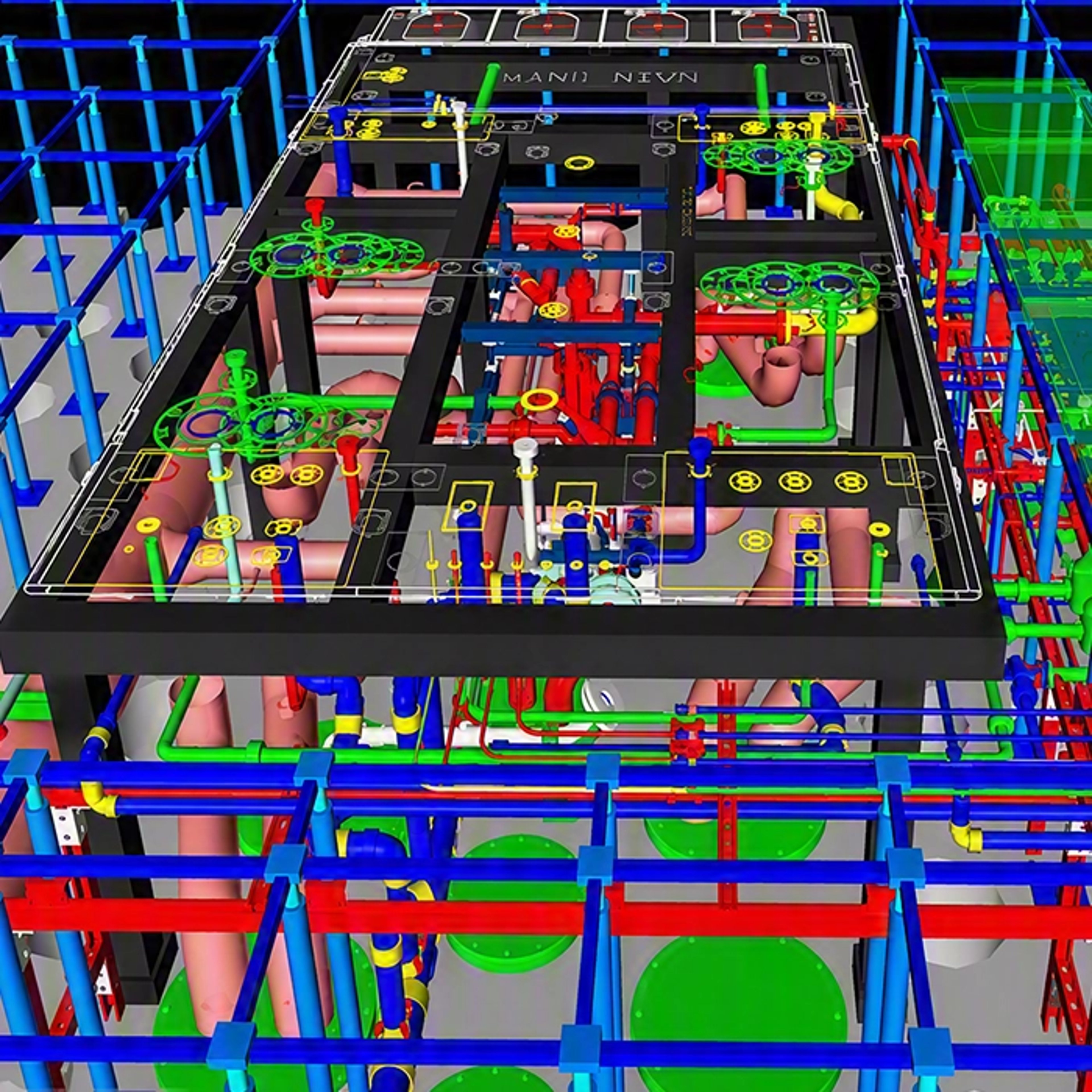
The project supported one of the world's most advanced semiconductor research initiatives and included infrastructure required for High-NA EUV lithography technology. Exentec delivered bulk gas systems, chemical systems, drains, and process mechanical infrastructure within a highly specialized cleanroom environment. Extensive VDC planning and constructability analysis enabled successful execution within a complex, active research campus undergoing significant expansion.
The challenge
A leading semiconductor research organization required the installation of highly specialized process utility and mechanical infrastructure to support a next-generation semiconductor research facility. The project required integration of complex bulk gas, chemical, drainage, and process utility systems within an active research campus while maintaining ongoing operations and coordinating with multiple stakeholders, contractors, and concurrent expansion projects.
Exentec's solution
Exentec utilized advanced Virtual Design and Construction (VDC), stakeholder coordination, and specialized semiconductor expertise to deliver the project's process mechanical scope. Working within an operational semiconductor research environment, the team coordinated closely with project leadership and multiple trades to install process mechanical, bulk gas, chemical, and utility systems safely and efficiently while meeting demanding technical and schedule requirements.
The results
Exentec successfully delivered critical infrastructure supporting advanced semiconductor research and next-generation lithography capabilities. Through detailed planning, technical expertise, and multidisciplinary coordination, the project maintained alignment with facility requirements while supporting one of the most important semiconductor innovation programs in the United States. The completed infrastructure provides the foundation for future semiconductor process development and research activities.
Experience that delivers
- Multi-million Euros of semiconductor research infrastructure delivered
- 24,000+ linear feet of systems modeled through advanced VDC execution
- Infrastructure installed to support High-NA EUV lithography technology, one of the most advanced chip manufacturing technologies available